


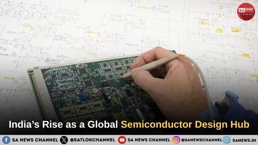
India’s technology journey is entering a new chapter as the country strengthens its position in global semiconductor design. For years, India was widely recognized for software services, IT talent, and its enormous technology market. Today, its role is expanding toward chip design, semiconductor research, engineering, packaging, and electronics manufacturing. Government-backed initiatives, global investments, startups, universities, and a large engineering workforce are contributing to this transition. Recent developments, including new semiconductor investments and expanding design capabilities, indicate that India is building a broader chip ecosystem rather than focusing on manufacturing alone. This transformation could influence AI, electric vehicles, telecommunications, consumer electronics, and future digital infrastructure.
- India’s Semiconductor Design Journey
- Why Chip Design Matters
- Government Support and the Semiconductor Mission
- Global Companies Are Expanding Their Indian Footprint
- The Rise of Indian Semiconductor Startups
- Opportunities Across AI, EVs and Electronics
- Challenges India Still Needs to Address
- India’s Changing Role in the Global Chip Industry
- Technology, Human Welfare, and Ground-Level Social Reform: The Path of True Knowledge
- FAQ on Semiconductor Startups
India’s Semiconductor Design Journey
India’s semiconductor story did not begin with the recent manufacturing push. For decades, multinational technology companies have used Indian engineering centres for semiconductor design, verification, embedded systems, software development, and research.
India’s large pool of engineers has become one of its major advantages. Recent industry reporting indicates that India already accounts for a significant share of global chip-design talent, while semiconductor-focused Global Capability Centres continue to expand. A 2026 Careernet analysis identified more than 110,000 professionals across the semiconductor GCC ecosystem it studied, with strong demand for VLSI and software roles.This existing design capability provides a foundation for the country’s next ambition: creating more intellectual property, products, startups, and commercially successful chips from India.
Why Chip Design Matters
From Engineering Services to Semiconductor IP
Designing a semiconductor involves much more than drawing circuits. Engineers work on architecture, verification, physical design, testing, software integration, and electronic design automation (EDA).India’s chip design ecosystem is increasingly important because design creates intellectual property (IP) that can be used across products and markets. The government’s Design Linked Incentive (DLI) Scheme provides financial incentives and design infrastructure support for areas including integrated circuits, chipsets, System-on-Chip (SoC) products, systems and IP cores.
The objective is therefore broader than simply producing chips. It is also about encouraging Indian companies and startups to develop semiconductor technologies that can eventually reach global markets.
Government Support and the Semiconductor Mission
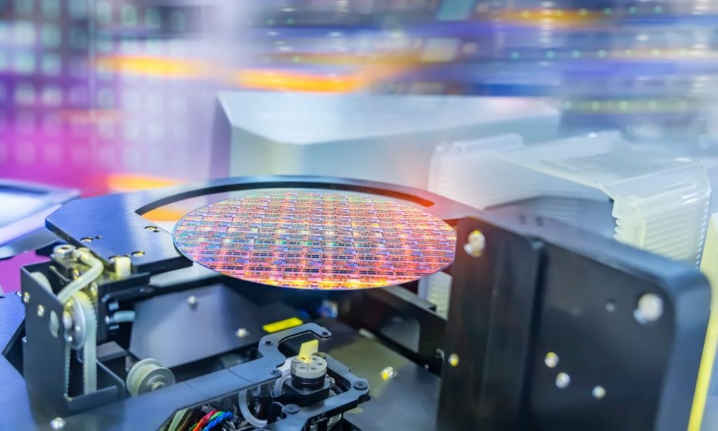
India has been building its semiconductor strategy through the India Semiconductor Mission, financial incentives, talent-development programs, and initiatives supporting chip design.The recent Semicon India 2026 event highlighted the growing scale of the ecosystem. Reuters reported that Applied Materials announced plans to invest $5 billion in India over the next decade, while India has approved semiconductor projects involving major investments.
Also Read: Who Controls AI? The Global Battle Over Artificial Intelligence Regulation
The government has also moved toward a broader ecosystem approach. Recent reports on Semicon 2.0 indicate that investment proposals are extending beyond fabrication into equipment, materials, gases, chemicals, substrates, and other parts of the semiconductor supply chain.This matters because a successful semiconductor industry requires many connected capabilities rather than a single factory.
Global Companies Are Expanding Their Indian Footprint
India’s growing importance is also reflected in the presence of international semiconductor companies and technology firms.Global players are investing in research, engineering, manufacturing support, packaging, equipment, and supply-chain capabilities. Renesas, for example, is involved in semiconductor packaging operations in Gujarat through its relationship with CG Semi, while other major companies are increasing their Indian presence.Such activity can create opportunities for Indian engineers, suppliers, startups, universities, and technology researchers. It can also help transfer technical knowledge and connect India more closely with global semiconductor value chains.
The Rise of Indian Semiconductor Startups
One of the most important developments is the growing interest in semiconductor startups.Startups can focus on specialized areas such as AI accelerators, automotive chips, IoT processors, power electronics, communication technologies, and security solutions. According to recent industry analysis, more than 100 startups are engaged in chip development as India attempts to convert its engineering strength into indigenous semiconductor products and IP.
However, turning a chip concept into a commercial product can take years and requires substantial technical expertise and capital. Talent remains a major challenge. Recent comments from Cadence highlighted the difficulty Indian chip startups face in finding people with experience across design, verification, and the wider chip-development process.
Opportunities Across AI, EVs and Electronics
The semiconductor opportunity extends far beyond smartphones and computers.Artificial intelligence, data centres, electric vehicles, industrial automation, telecommunications, defence electronics, and connected devices all require increasingly sophisticated semiconductor technologies.India’s huge domestic electronics market can provide an important testing ground for innovation. At the same time, globally competitive products could allow Indian semiconductor companies to sell beyond the domestic market.The combination of AI chip design, automotive semiconductors, 5G and 6G technologies, IoT chips, and advanced packaging could therefore create multiple growth pathways.
Challenges India Still Needs to Address
India’s semiconductor ambitions also face significant challenges.
Talent and Advanced Skills
The industry needs specialists in VLSI, chip architecture, verification, fabrication, packaging, materials science, semiconductor equipment, and EDA tools. Building this talent base requires sustained cooperation between universities and industry.
Global Supply Chains
Semiconductors depend on highly interconnected global supply chains. India cannot immediately localize every material, tool, technology, or manufacturing process.
Recent industry discussions have emphasized supply-chain resilience, cybersecurity, diversified suppliers, and stronger domestic capabilities in design, fabrication, EDA, and packaging.
Moving From Design to Commercial Products
India’s established design expertise is a major foundation, but the next challenge is developing globally competitive semiconductor products and intellectual property. This requires long-term research, patient capital, strong testing infrastructure, and close industry-academia collaboration.
India’s Changing Role in the Global Chip Industry
India is not yet a fully self-sufficient semiconductor manufacturing power, and large-scale fabrication remains a major undertaking. However, the country’s semiconductor story is no longer limited to being a large consumer of imported technology.Its growing capabilities in semiconductor design, engineering, research, startups, packaging, electronics manufacturing, and supply-chain development are changing its position within the global industry.
The opportunity is particularly significant because India already possesses several important ingredients: a large technology workforce, a huge domestic market, expanding digital infrastructure, research institutions, entrepreneurial talent, and increasing international partnerships.If these strengths are developed together, India could become an increasingly important contributor to the global semiconductor ecosystem-not only as a consumer or engineering-services destination, but also as a source of semiconductor IP, products, and innovation.
Technology, Human Welfare, and Ground-Level Social Reform: The Path of True Knowledge
As India strengthens its position in chip design and core technology, it is essential to recognize that the true purpose of technological innovation should be human and societal well-being. The teachings and public welfare initiatives led by Sant Rampal Ji Maharaj remind us that genuine knowledge (gyaan) is that which directly solves real-world human challenges.
While the nation advances digitally and scientifically, widespread social and ground-level transformations are taking place under the guidance of Sant Rampal Ji Maharaj. Under the ‘Annapurna Muhim’, underprivileged, helpless, and differently-abled families are being provided with permanent shelter (pukka homes), food, monthly groceries, clothing, and medical care.
For farmers, relief from waterlogging is provided through free motor pumps, pipelines, seeds, and fertilizers. Simultaneously, under the ‘Gau Suraksha Muhim’, free green and dry fodder, large tin-sheds, fodder storage facilities, and clean drinking water are being supplied to gaushalas across the country. In addition, dowry-free mass marriages (Ramaini), anti-addiction drives, and the creation of a caste-free, harmonious society are restoring hope to countless lives.
Whether it is semiconductor technology or any scientific advancement, innovation achieves its true significance only when aligned with high moral values, empathy, and selfless service (sewa). Blending modern technology with the direction of knowledge and service shown by Sant Rampal Ji Maharaj can play a vital role in building a strong, prosperous, and addiction-free society.
FAQ on Semiconductor Startups
1. Why is India becoming important in semiconductor design?
India has a large pool of skilled engineers, growing semiconductor startups, strong technology companies, and increasing government support for chip design and innovation.
2. What is semiconductor design?
Semiconductor design is the process of creating the architecture, circuits, and layout of computer chips before they are manufactured.
3. What is India’s Design Linked Incentive Scheme?
The Design Linked Incentive Scheme supports semiconductor design companies and startups through financial incentives and infrastructure support for chip and semiconductor IP development.
4. Which industries can benefit from India’s semiconductor growth?
AI, electric vehicles, telecommunications, consumer electronics, data centres, IoT, automotive technology, and industrial automation can benefit from semiconductor growth.
5. Can India become a major global semiconductor hub?
India is developing capabilities in chip design, manufacturing, packaging, research, and supply chains. Continued investment, skilled talent, infrastructure, and innovation will shape its future role in the global semiconductor industry.